Product Description: CD4015 SOP – Dual 4-Bit Serial-In/Parallel-Out Shift Register
The CD4015 SOP Dual 4-Bit Serial-In/Parallel-Out Shift Register is a CMOS-based integrated circuit designed to provide data storage and shifting capabilities in a dual 4-bit shift register configuration. This IC contains two independent shift registers, each capable of receiving serial data on a single input (serial-in) and outputting it in parallel through 4-bit outputs. The CD4015 is ideal for applications that require data conversion, storage, and shifting between serial and parallel formats.
In a shift register configuration, data is shifted from one bit to the next on each clock pulse, allowing for serial-to-parallel conversion or parallel-to-serial conversion depending on the specific circuit design. The CD4015 uses serial input (SI) to feed data into the register, while the parallel output provides access to the stored data at once, making it highly useful in data transfer and bit manipulation tasks.
Built using CMOS technology, the CD4015 provides low power consumption and excellent noise immunity, making it suitable for battery-powered devices and noisy environments. The SOP-16 package ensures a compact form factor, ideal for integration into surface-mount systems (SMT) and modern PCB designs.
Key Features:
- Dual 4-Bit Shift Registers: The IC features two independent 4-bit shift registers, allowing for efficient data storage and shifting in dual channels.
- Serial-In/Parallel-Out Operation: The CD4015 converts serial data input into parallel outputs. This allows for efficient data transfer from serial devices to parallel devices.
- Clocked Operation: The shift registers are clocked on the rising edge of the clock input, making it easy to synchronize the shifting operation with external systems.
- Asynchronous Reset: The reset pin allows for asynchronous clearing of the register, setting all outputs to LOW (0), useful for initialization or error recovery.
- Low Power Consumption: The CMOS technology ensures low power consumption, making the CD4015 suitable for battery-operated and low-power systems.
- Wide Operating Voltage: The IC operates over a voltage range of 3V to 18V, making it compatible with both low-voltage and standard logic systems.
- Compact SOP-16 Package: The SOP-16 package offers a small footprint, making it ideal for surface-mount applications and space-constrained PCB designs.
Applications:
- Data Conversion: The CD4015 is widely used in serial-to-parallel conversion or parallel-to-serial conversion, making it ideal for applications where data needs to be transferred between serial communication systems (such as UART, SPI, or I2C) and parallel devices (such as data buses or registers).
- Signal Processing: The shift register can be used in signal processing applications, where bit manipulation or bit shifting is required to manipulate data streams or control signals in digital systems.
- Data Storage: The CD4015 can store data in parallel format and shift it out serially, making it useful in memory systems or for storing intermediate data in digital computing circuits.
- Timing Circuits: It can be used to build timing circuits that require shifting operations to occur at precise intervals, such as in pulse counting or clock division systems.
- Control Systems: The CD4015 can be integrated into digital control systems to manage the flow of data between components, sensors, and actuators. It is particularly useful in systems that require bit-level data management.
- Data Communication: In communication systems, the CD4015 can be used for data buffering, where serial data is received and output in parallel format to multiple components or buses.
- LED Displays and Indicators: The CD4015 can be used to control LED displays, where data is serially input and then displayed in parallel across multiple segments or rows.
- Digital Signal Routing: In digital signal routing applications, the shift register can be used to route data or control signals in parallel paths, shifting them serially when necessary.
Package Included:
1 x CD4015 SOP Dual 4-Bit Serial-In/Parallel-Out Shift Register
Please note that the product image is for illustrative purposes only. The actual product may vary slightly in appearance.
 TL082CP DIP -18V 200mA Dual Operational Amplifiers
1 × රු20.00
TL082CP DIP -18V 200mA Dual Operational Amplifiers
1 × රු20.00  TDA8920TH 2 x 50W Class D Power Amplifier IC
1 × රු1,820.00
TDA8920TH 2 x 50W Class D Power Amplifier IC
1 × රු1,820.00  CD4024 DIP 7-Stage Binary Ripple Counter IC
1 × රු77.00
CD4024 DIP 7-Stage Binary Ripple Counter IC
1 × රු77.00  2SC2577 TO-3Pin 120V 8A NPN Transistor
1 × රු286.00
2SC2577 TO-3Pin 120V 8A NPN Transistor
1 × රු286.00 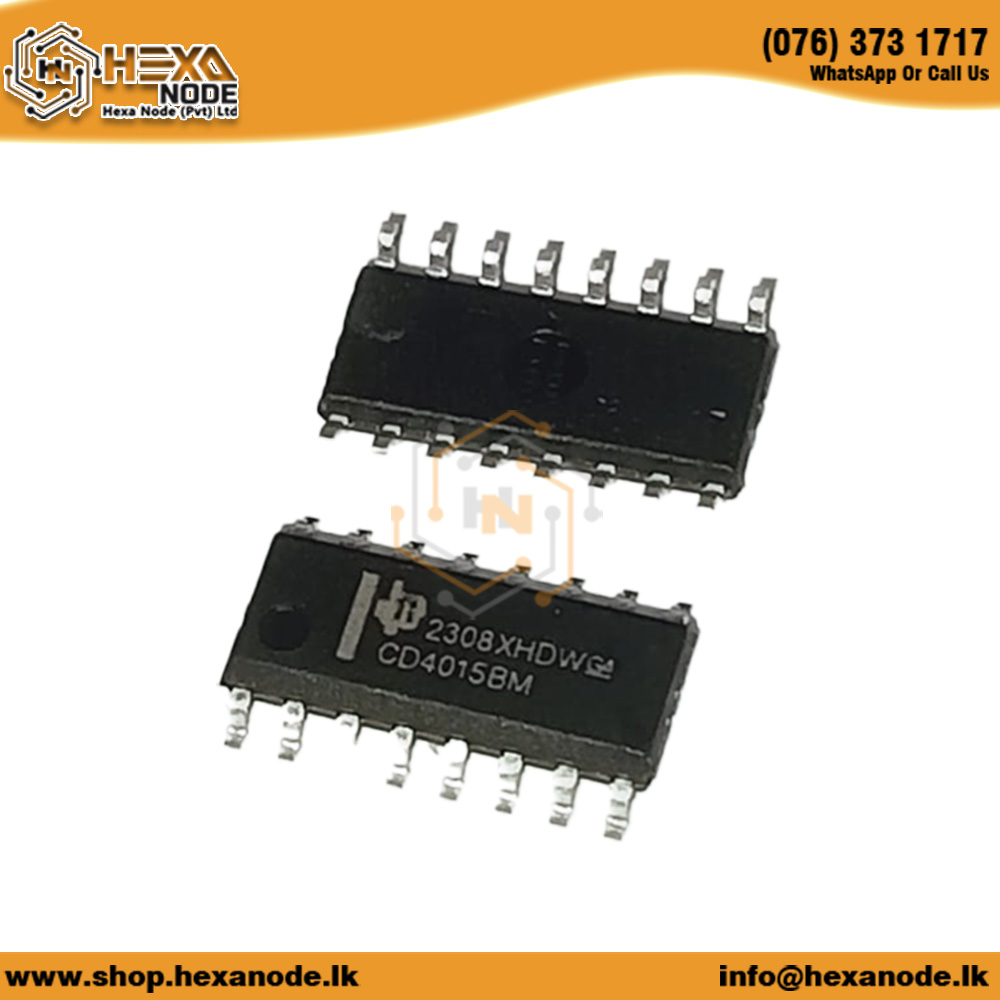
There are no reviews yet.